Samsung Develops World’s First 6th-Generation HBM: HBM4 with 4nm Logic Chip Design
Samsung Develops World’s First 6th-Generation HBM: HBM4 with 4nm Logic Chip Design
- Why Enterprise RAID Rebuilding Succeeds Where Consumer Arrays Fail?
- Linus Torvalds Rejects MMC Subsystem Updates for Linux 7.0: “Complete Garbage”
- The Man Who Maintained Sudo for 30 Years Now Struggles to Fund the Work That Powers Millions of Servers
- How Close Are Quantum Computers to Breaking RSA-2048?
- Why Windows 10 Users Are Flocking to Zorin OS 18 Instead of Linux Mint?
- How to Prevent Ransomware Infection Risks?
- What is the best alternative to Microsoft Office?
Samsung Develops World’s First 6th-Generation HBM: HBM4 with 4nm Logic Chip Design
Samsung has reached a significant milestone in high-bandwidth memory (HBM) technology by completing the logic chip design for its next-generation HBM4 memory.
According to South Korean media outlet Chosun Ilbo, Samsung’s Device Solutions (DS) division, responsible for memory, recently finalized the logic chip design.
The foundry division has already initiated trial production using a 4nm process. Following final performance validation of the logic chip, Samsung plans to provide HBM4 samples for further testing.

The Role of the Logic Chip in HBM Stacks
The logic chip, also known as the Logic Die or Base Die, functions as the “brain” of the HBM stack. It controls the multiple layers of DRAM chips stacked on top of it. Heat management is a critical challenge in HBM operation, as the logic chip is the main heat generator within the stack. Employing an advanced 4nm process significantly enhances both the power efficiency and performance of HBM4.
In addition to utilizing a 4nm process for its logic chip, Samsung has adopted a 10nm process for the DRAM layers in HBM4.
Evolution and Capabilities of High-Bandwidth Memory
High-Bandwidth Memory (HBM) is designed for applications such as high-performance computing (HPC), artificial intelligence (AI), and graphics processing units (GPUs). By addressing bandwidth and power consumption bottlenecks, HBM is a cornerstone for enabling cutting-edge computational tasks.
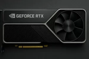
HBM leverages 3D stacking technology, which vertically stacks multiple DRAM chips. Using through-silicon via (TSV) technology, HBM facilitates high-speed signal transmission between chips, significantly reducing data transfer distance and latency. This architecture provides exceptionally high bandwidth, making it ideal for processing-intensive tasks alongside GPUs, such as those in NVIDIA’s latest AI chips.
HBM technology has evolved through six generations: HBM, HBM2, HBM2e, HBM3, HBM3e (an extended version of HBM3), and now HBM4. Each successive generation has delivered significant improvements in bandwidth, capacity, and energy efficiency:
- HBM1 introduced 128GB/s bandwidth, marking the beginning of high-bandwidth memory applications.
- Later generations, including HBM3 and HBM3e, have significantly increased performance.
Breakthroughs in HBM4 Performance
Industry data shows that the HBM4 standard supports a 2048-bit interface and a data transfer rate of 6.4 GT/s. A single HBM4 stack achieves an impressive bandwidth of 1.6 TB/s, representing a major leap from the capabilities of HBM3E. This enhanced performance supports the growing demands of AI, deep learning, big data processing, and HPC.
The HBM4 generation includes configurations with 12-layer (12Hi) and 16-layer (16Hi) stacks, building on the advancements seen in HBM3e’s 8-layer and 12-layer designs.
Samsung’s HBM Strategy and Roadmap
In Q3 2023, Jaejune Kim, Executive Vice President of Samsung’s memory division, revealed that the company’s HBM sales had increased by over 70% quarter-on-quarter. Production and sales of HBM3E with 8-layer and 12-layer stacks were underway, with HBM3E accounting for approximately 10% of Samsung’s total HBM sales at the time. Kim projected that HBM3E would make up 50% of HBM sales by Q4 2023.
Samsung’s development of HBM4 is proceeding on schedule, with plans for mass production to commence in the second half of 2025.
HBM4’s introduction signals a transformative step in memory technology, catering to the ever-increasing performance demands of AI and HPC.
What are Key Differences Between HBM4 and DDR5 Chips?
High-Bandwidth Memory (HBM) and DDR5 are both advanced DRAM technologies, but they are designed for different purposes and differ in architecture, performance, and applications. Here’s a comparison based on their key features:
1. Architecture
-
HBM4:
- 3D-Stacked Design: HBM4 uses a 3D stacking architecture, with multiple DRAM dies stacked vertically. These layers are interconnected by Through-Silicon Via (TSV) technology, enabling extremely high data transfer speeds.
- Close Proximity to Processors: HBM4 sits directly on top of the processor substrate, reducing latency and power consumption.
- Logic Die Integration: It includes a logic die to manage data flow and optimize performance within the stack.
-
DDR5:
- 2D Planar Design: DDR5 modules are planar (flat) and packaged into DIMMs that are connected to the motherboard via traditional memory slots.
- Off-Chip Controller: DDR5 relies on a separate memory controller housed within the CPU or chipset for operation.
2. Performance and Bandwidth
-
HBM4:
- Offers ultra-high bandwidth, with each stack capable of achieving up to 1.6 TB/s, thanks to a 2048-bit wide memory interface and data rates of 6.4 GT/s.
- Designed for tasks demanding immense data throughput, such as AI, deep learning, HPC, and GPU acceleration.
-
DDR5:
- DDR5’s data rates range between 4.8 to 8.4 GT/s, but its narrower interface (usually 64 bits) results in lower bandwidth compared to HBM.
- Suitable for consumer PCs, servers, and workloads with standard memory demands.
3. Power Efficiency
-
HBM4:
- Delivers better power efficiency due to its proximity to the processor and use of advanced manufacturing processes like 4nm (logic chip) and 10nm (DRAM chip).
- The TSV and 3D stack significantly reduce signal distance, cutting power consumption for data transfers.
-
DDR5:
- While DDR5 introduces improved power management via on-module PMIC (Power Management IC) and lower operating voltages (1.1V compared to 1.2V in DDR4), its energy efficiency per bandwidth is still lower than HBM technology.
4. Capacity
-
HBM4:
- Each HBM4 stack offers higher individual capacity due to its 12-Hi (12 DRAM layers) or 16-Hi (16 layers) design, scaling well for memory-intensive applications.
- Total capacity can reach tens of gigabytes per stack, though multiple stacks are often used together.
-
DDR5:
- Single DIMMs can provide up to 512GB per module in the future, leveraging advancements like dual sub-channels, though this is less efficient for specialized workloads requiring ultra-high speed and parallelism.
5. Applications
-
HBM4:
- Designed for high-performance, specialized applications such as:
- AI and machine learning workloads.
- GPU acceleration.
- HPC simulations.
- Real-time analytics and big data processing.
- HBM is typically used in GPUs (like NVIDIA’s AI processors), advanced accelerators, and custom solutions.
- Designed for high-performance, specialized applications such as:
-
DDR5:
- Primarily for general-purpose computing, including:
- Consumer desktops and laptops.
- Enterprise and cloud servers.
- Gaming and multimedia applications.
- Primarily for general-purpose computing, including:
Summary
| Feature | HBM4 | DDR5 |
|---|---|---|
| Design | 3D stacked, TSV | Planar DIMM |
| Bandwidth | Up to 1.6 TB/s per stack | 4.8–8.4 GT/s |
| Power Efficiency | Very high (per bit) | Improved but lower |
| Applications | Specialized AI/HPC tasks | General-purpose memory |
| Capacity | Smaller but stackable | Larger DIMM capacities |
Overall, HBM4 outperforms DDR5 in bandwidth, latency, and energy efficiency, making it ideal for cutting-edge, high-performance applications. In contrast, DDR5 focuses on scalability and affordability for broader use cases in mainstream and server environments.