Russia Homegrown Lithography Machine: Costing Less Than US$54K
Latest Developments in Russia Homegrown Lithography Machine: Less Than US$54K
- 60% of MD5 Password Hashes Can Be Cracked in Under an Hour with a Single GPU
- Dirty Frag: Root Access on Every Major Linux Distribution — No Patch, No Warning
- Ubuntu 26.04 LTS (Resolute Raccoon): The Most Ambitious Ubuntu LTS in a Decade
- Proton Mail: Data Transferred to FBI Again!
- How Close Are Quantum Computers to Breaking RSA-2048?
- How to Prevent Ransomware Infection Risks?
- What is the best alternative to Microsoft Office?
Latest Developments in Russia Homegrown Lithography Machine: Less Than US$54K
Russia’s domestically developed lithography machine has seen new advancements.
According to reports from the Russian media outlet cnews, a lithography complex has been established in Saint Petersburg, which includes equipment for maskless image acquisition on substrates and silicon plasma etching.
Developers claim that the first machine for maskless nanolithography costs around 5 million rubles (about US$53,636.55), while similar foreign products are valued at several billion rubles.
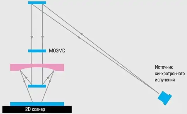
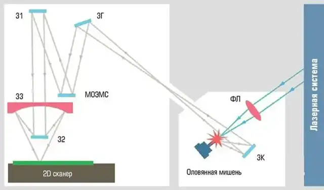
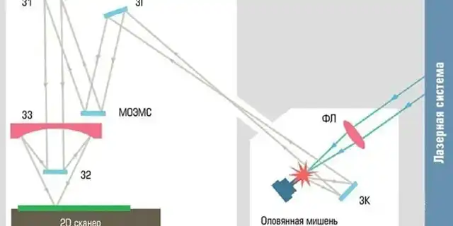
X-Ray Lithography Technology
As early as April last year, Russian media reported that the Moscow Institute of Electronics and Technology (MIET) had undertaken a lithography machine project for chip manufacturing, with an initial investment of 670 million rubles (approximately 51 million RMB) from the Russian government. The lithography machine under development aims to achieve EUV-level capabilities, but with a completely different technological principle, based on a synchrotron accelerator and/or plasma source for maskless X-ray lithography.
Currently, only ASML is capable of developing and manufacturing EUV lithography machines globally, but their technology has limitations. Russia plans to develop an entirely new EUV lithography machine using X-ray technology, eliminating the need for photomasks in chip production.
Lithography machine architecture and technology are quite complex, but the primary factors determining lithography machine resolution are three: the constant K, the wavelength of the light source, and the numerical aperture of the objective lens. The shorter the wavelength, the higher the resolution. Current EUV lithography machines use extreme ultraviolet light with a 13.5nm wavelength and can be used for advanced processes down to 7nm and below.
X-ray lithography machines use X-rays with wavelengths ranging from 0.01nm to 10nm, even shorter than EUV, resulting in much higher lithographic resolution.
Additionally, X-ray lithography machines have another advantage over current EUV lithography machines – they don’t require photomasks and can directly write lithography, saving a substantial amount of cost.
Due to these two characteristics, the Russian-developed X-ray lithography machine is being hailed as having significant advantages, even claimed by local media as a lithography machine that the world does not have, something ASML cannot achieve.
From available information, it is indeed true that there is no globally scalable X-ray lithography machine for mass production. However, this technology is not new; it has been researched not only in the United States and Europe but also by domestic research institutions in China. The difference lies in the efficiency of chip production, which cannot compete with ASML lithography machines and is only suitable for specific scenarios.
Russia’s Latest Advancements in Lithography
Experts from Saint Petersburg’s Peter the Great St. Petersburg Polytechnic University (SPbPU) have announced that Russia has developed two devices for producing nanoscale microelectronic structures. This could potentially address Russia’s technological sovereignty issues in microelectronics.
According to the developers, X-ray lithography machines are significantly more cost-effective in terms of both money and time compared to traditional lithography technologies because traditional lithography requires specialized masks to create images. X-ray lithography machines, on the other hand, can produce chips without the need for photomasks.
The estimated cost of such equipment is around 5 million rubles, which is comparable to the price of many conventional cars. The organization claims that the cost of similar foreign devices falls between 10 to 13 billion rubles.
This complex, developed under the leadership of SPbPU, aims to create nanoscale structures required for various microelectronic devices. The first stage focuses on developing X-ray lithography machines, while the second stage is dedicated to developing equipment for silicon plasma chemical etching.
The head of the project mentioned that films created using this facility surpass those produced using liquid or laser etching in terms of reliability and sensitivity. It’s emphasized that these are entirely domestically produced products.
The cost of the Russian-developed etching machine has not been disclosed.
Artem Osipov, the head of the “Materials Technology” laboratory at Saint Petersburg Polytechnic University, stated that in addition to the two devices within the complex developed internally at the university, there is research into extending the lifespan of radar equipment by more than 20 times. This research could potentially reduce the weight and size of solar panels and make them operate efficiently even on overcast days.
It is not specified whether any Russian chip manufacturers have shown interest in the new installation. As of now, there is no news regarding when these technologies will be put into practical production. Meanwhile, the inventors continue to improve their lithography complex, with plans to equip two of the devices with artificial intelligence, although the specific tasks they will solve have not been detailed.
Saint Petersburg Polytechnic University is not the only Russian institution striving to create advanced lithography solutions.
Another Backup: Lithography Machine Capable of Producing 7nm Chips by 2028
In addition to the X-ray lithography machine, as early as October 2022, CNews reported that the Novgorod Applied Physics Research Institute of the Russian Academy of Sciences (IPF RAS) was actively researching a lithography machine capable of producing 7nm chips.
According to the report from that time, IPF RAS in Novgorod was developing Russia’s first lithography device for producing ultrasmall nanoelectronic devices. By October 2022, scientists at RAS had created the first device demonstration sample. This device allows the acquisition of individual images with a resolution of up to 7nm on substrates.
It was stated that IPF RAS planned to create an industrial prototype of a domestically-produced 7nm lithography machine within six years. This “Alpha machine” is expected to be created by 2024 and become a working device capable of performing full operational cycles.
In the second phase, the “test machine” is set to appear in 2026. According to Novgorod’s strategic website, the device system will be improved, more complex, with increased resolution, productivity, and many operations being automated. This device can be used for large-scale production.
In the third phase, from 2026 to 2028, Russian domestic lithography machines will have more powerful radiation sources, improved positioning and feed systems, and will begin full-scale operations.
Nikolai Chkhalo, Deputy Director of the Institute of Microstructure Physics at the Russian Academy of Sciences, mentioned that the optical system of the demonstrator exceeds all similar devices worldwide. He pointed out that the radiation source in the Novgorod model operates more compactly compared to ASML’s lithography machines. According to him, under the same radiation source power, the efficiency of the Russian machine will be 1.5 to 2 times higher than ASML’s.
It is well-known that as of October 2023, Russia is unable to produce microcircuits using modern technology; the country can only use 65nm structures, which are obsolete as of almost 20 years ago. Russia is currently constructing a 28nm factory, but this technology is also outdated. State-of-the-art chips globally have already reached 4nm and are transitioning to 3nm in 2023.
As described, IAP RAS is working to close the substantial gap between Russia and other countries worldwide. University experts are developing Russia’s first lithography machine capable of producing 7nm chips. However, it
will take several years, and the equipment may not be fully operational until 2028.
Homegrown Lithography Materials
Similarly, in March 2023, CNews reported that the Russian Ministry of Industry and Trade had ordered the development of lithography materials for microelectronics production, particularly the production of lithography materials, including photoresists with a laser radiation wavelength of 248nm.
This work, designated under the “Photolysis” code, was initiated due to the absence of such materials being developed and produced in Russia.
As part of this research work ordered by the Ministry of Industry and Trade, plans include the manufacturing of photoresists for lithography processes, namely FR248-01, FR248-02, FR248-03, FR248-04, FR248-05 brands, and two anti-reflective coatings, PA248-01 and PA248-02.
Contractors are not only required to perform theoretical and experimental work but also to test experimental batches of photoresists and prepare for their production. The document states, “During the research, it is necessary to transfer samples of the developed materials to enterprises and draw conclusions about the parameter level and applicability.”
The use of foreign materials and equipment during the research and development process must be approved by the Ministry of Industry and Trade.
For Russia, any of these endeavors are no simple tasks.