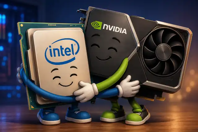
Intel & NVIDIA Forge Historic Alliance — Jensen Huang Receives Honorary Doctorate at Carnegie Mellon
Intel & NVIDIA Forge Historic Alliance — Jensen Huang Receives Honorary Doctorate at Carnegie Mellon
- 60% of MD5 Password Hashes Can Be Cracked in Under an Hour with a Single GPU
- Dirty Frag: Root Access on Every Major Linux Distribution — No Patch, No Warning
- Ubuntu 26.04 LTS (Resolute Raccoon): The Most Ambitious Ubuntu LTS in a Decade
- Proton Mail: Data Transferred to FBI Again!
- How Close Are Quantum Computers to Breaking RSA-2048?
- How to Prevent Ransomware Infection Risks?
- What is the best alternative to Microsoft Office?
Intel & NVIDIA Forge Historic Alliance — Jensen Huang Receives Honorary Doctorate at Carnegie Mellon
As NVIDIA’s CEO accepts a prestigious degree from Carnegie Mellon University, Intel’s Lip-Bu Tan reaffirms a sweeping partnership that spans AI data centers, consumer SoCs, and chip manufacturing — with far-reaching implications for the semiconductor industry.
A Ceremony That Made Industry History
Carnegie Mellon University’s 128th Commencement ceremony on Sunday, May 10, 2026, was already a landmark occasion — conferring degrees on more than 5,800 graduates. But it was a moment on the honorary stage that sent ripples through the global semiconductor industry: NVIDIA founder and CEO Jensen Huang received an honorary Doctor of Science and Technology degree, CMU’s highest distinction, conferred by university president Farnam Jahanian.
Intel CEO Lip-Bu Tan was present for the occasion and placed the doctoral hood upon Huang — a gesture of personal congratulation from the leader of one of NVIDIA’s closest new partners. Tan swiftly took to social media to announce that the two companies are actively collaborating on “exciting new products,” signaling that their landmark cooperation agreement, struck in late 2025, is advancing at pace.
In his commencement address, Huang called Carnegie Mellon “one of the true birthplaces of artificial intelligence and robotics,” and urged graduates to embrace the transformative moment they are entering. “A new industry is being born. A new era of science and discovery is beginning,” he said.
- NVIDIA invested $5 billion in Intel common stock at $23.28 per share as part of a comprehensive strategic agreement announced in late 2025.
- The two companies are jointly developing a custom Xeon processor fully integrated with NVIDIA’s NVLink high-speed interconnect technology, targeted at AI data centers.
- A consumer SoC codenamed “Serpent Lake” — expected around 2028–2029 — is set to become the first Intel chip to integrate NVIDIA RTX GPU IP, according to industry leaks.
- NVIDIA’s next-generation “Feynman” GPU architecture is reportedly set to use Intel’s EMIB advanced packaging technology for I/O dies, alongside continued TSMC production for core compute dies.
- Entry-level and mid-range gaming graphics cards may also be manufactured using Intel’s 18A-P or 14A process nodes.
Data Centers: A Custom Xeon Built for NVIDIA
At the heart of the Intel–NVIDIA enterprise strategy is a co-developed Xeon processor designed exclusively for NVIDIA’s AI infrastructure platforms. Intel has confirmed it will supply NVIDIA directly — not through third-party hyperscalers — with a custom x86 CPU that integrates NVIDIA’s NVLink Fusion interconnect technology.
This arrangement allows Intel’s x86 architecture to slot directly into NVIDIA’s AI server racks alongside Blackwell and the forthcoming Rubin GPU generations, enabling high-bandwidth CPU-to-GPU communication that previously required proprietary Arm-based solutions such as NVIDIA’s own Grace and Vera CPUs. For Intel, it represents a crucial foothold in the booming AI infrastructure market.
— John Pitzer, Intel VP of Corporate Planning & Investor Relations
Consumer Market: “Serpent Lake” and the RTX-Powered SoC
On the consumer side, the most anticipated product is a chip codenamed “Serpent Lake” — a mobile-first SoC that industry leakers describe as a branch of Intel’s future Titan Lake CPU architecture, paired with NVIDIA RTX GPU chiplets fabricated on a TSMC 3nm-class process. The integrated package is expected to support 16 channels of LPDDR6 memory, addressing one of the key bandwidth bottlenecks that have hampered rival integrated GPU designs.
If the leaks prove accurate, Serpent Lake would launch around 2028–2029 and mark the first time an Intel consumer chip ships with NVIDIA GPU silicon inside the package — a significant competitive move against AMD’s integrated APU lineup, which has grown dominant in the high-performance laptop segment. Intel will produce and distribute the RTX-powered SoCs; NVIDIA will contribute GPU chiplet IP and its broader software and AI stack, including CUDA.
It is important to note that the “Serpent Lake” codename, specific core counts, and architectural details remain based on leaks from hardware analysts rather than confirmed Intel or NVIDIA roadmaps, and should be treated as subject to change.
Manufacturing Partnership: Feynman Comes to Intel Foundry
The third pillar of the collaboration — and the one attracting the most attention from supply-chain analysts — is NVIDIA’s decision to use Intel’s foundry capabilities for its next-generation “Feynman” GPU architecture, expected in 2028.
According to reports from DigiTimes and corroborated by multiple industry sources, the core GPU compute dies for Feynman will continue to be manufactured by TSMC, likely on its advanced A16 process. However, the I/O dies will partially adopt Intel’s 18A or 14A process nodes, and Intel’s proprietary EMIB (Embedded Multi-die Interconnect Bridge) advanced packaging technology will be used for a portion of final assembly — with Intel’s share estimated at roughly 25% of total production volume.
The rationale is strategic: TSMC’s CoWoS advanced packaging capacity has consistently fallen short of NVIDIA’s voracious demand. By bringing Intel into the supply chain for non-core components, NVIDIA gains resilience without concentrating risk on a single foundry. For Intel, landing NVIDIA as a Feynman customer — even in a limited capacity — is a major validation of its foundry revival strategy under Lip-Bu Tan.
NVIDIA has not officially confirmed the specific manufacturing breakdown for Feynman, and Intel has not publicly acknowledged the arrangement beyond promoting its 18A, 14A, and advanced packaging capabilities as pillars of its foundry business.
A New Chapter for Silicon
The Intel–NVIDIA alliance represents a remarkable realignment in an industry long defined by fierce rivalry. For decades, the two companies competed for the same sockets in PCs and servers — Intel with integrated graphics and x86 dominance, NVIDIA with discrete GPUs and, more recently, AI accelerators. Their partnership signals that in the age of generative AI, specialization and collaboration may prove more valuable than competition.
For Lip-Bu Tan, the relationship with Jensen Huang — cemented today under the Pennsylvania sky at Carnegie Mellon — is a cornerstone of Intel’s broader turnaround. For Huang, it provides x86 expertise, manufacturing diversification, and a path to embedding NVIDIA intelligence deeper into the fabric of personal computing than ever before.