NAND Flash Is Racing Toward 1,000 Layers — and 32TB Consumer SSDs Could Follow After 2030
- Linux Kernel Removes strncpy After Six Years and 362 Patches
- Linux Kernel Drops 40-Year-Old AppleTalk Protocol — AI-Generated Patch Flood Was the Last Straw
- Apple’s Native Linux Container Tool Has Arrived — But Can It Really Replace Docker?
- 60% of MD5 Password Hashes Can Be Cracked in Under an Hour with a Single GPU
- Dirty Frag: Root Access on Every Major Linux Distribution — No Patch, No Warning
NAND Flash Is Racing Toward 1,000 Layers — and 32TB Consumer SSDs Could Follow After 2030
The defining metric in 3D NAND flash memory has always been layer count, and the industry’s two biggest players are now in an open sprint toward a four-figure number. SK Hynix and Samsung have each pushed past long-standing technical ceilings in the past year, and Samsung’s newest prototype suggests the long-rumored 1,000-layer chip is no longer just a roadmap slide.
Where things stand today
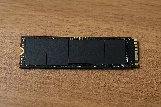
SK Hynix currently holds the mass-production record with its 321-layer 4D NAND, branded internally as part of its “4D” lineup, which began shipping in 2Tb QLC form for PC SSDs in 2026 after entering production in 2024-2025. Most NAND shipping today, however, still falls in the 200-to-300-layer range. Samsung, meanwhile, is preparing its 10th-generation V-NAND, which crosses the 400-layer mark, for mass production within the year — squarely aimed at closing the gap with its Korean rival.
The 900-layer leap
The more striking development came in late May, when Samsung disclosed a working 900-layer V-NAND prototype built using a technique it calls Cell Multi-Bonding, or CMB. Rather than etching one impossibly tall stack on a single wafer, Samsung manufactures two separate 450-layer cell arrays and fuses them together using hybrid bonding with embedded metal interconnects. Samsung says it has verified normal cell operation on the bonded chip, meaning it functions as a real memory device rather than a lab curiosity — though yield and manufacturing cost at commercial scale have not yet been demonstrated.
The approach exists because single-wafer stacking is running into hard physical limits: wafer warpage, alignment precision, and channel-hole etching depth all get harder as the stack gets taller. Samsung addressed warpage with a redesigned upper chuck system and tackled alignment errors with an updated overlay-correction process. Bonding two shorter, more manageable stacks sidesteps the problem of etching one extremely deep one.
| Company | Layer count | Status |
|---|---|---|
| SK Hynix | 321 layers (4D NAND, QLC) | Mass production, PC SSDs rolling out in 2026 |
| Samsung | 400+ layers (Gen10 V-NAND) | Mass production targeted this year |
| Samsung | 900 layers (two 450-layer dies via CMB bonding) | Verified prototype, not yet commercial |
| Industry-wide | 1,000+ layers | Targeted around 2030, likely later |
Why “around 2030” probably means later
Samsung’s own projection points to roughly 2030 for breaking the 1,000-layer mark by extending CMB bonding further once its 400-plus-layer single-stack generation matures. Industry watchers are generally more cautious than that. Getting from a verified 900-layer prototype to a shippable 1,000-layer product involves the unglamorous but essential work of fixing yield, taming manufacturing cost, and proving reliability at scale — the kind of engineering grind that routinely pushes semiconductor roadmaps a few years past their original target. A realistic reading is that the 1,000-layer milestone lands sometime after 2030 rather than precisely on it.
What it means for storage capacity
The payoff for clearing that bar is substantial. Today’s consumer M.2 SSDs using 200-plus-layer QLC flash top out around 8TB. Scaling that density up to 1,000 layers would put 32TB consumer drives within reach — enough that spinning hard drives would lose most of their remaining rationale for everyday use.
The enterprise and AI storage side is moving even faster in absolute terms. SanDisk has already demonstrated a 256TB enterprise NVMe SSD built on its UltraQLC platform, with rivals such as Micron and Solidigm fielding drives in a similar range. Layer counts climbing toward 1,000 — combined with continued QLC and eventual PLC cell-density gains — point toward single drives reaching petabyte-class capacity, around 1,000TB, within the next several years, well ahead of the consumer market hitting 32TB.
The price question
Density is not the same as affordability. Today’s high-capacity enterprise drives, like SanDisk’s 256TB model, are priced for hyperscale data centers, not home users, and bonded multi-die chips like Samsung’s 900-layer prototype are inherently more complex and costly to manufacture than a single-stack design. Unless NAND pricing and packaging costs fall substantially between now and the early 2030s, a 32TB consumer SSD may debut as a premium, even niche, product rather than a mainstream upgrade — at least at first.