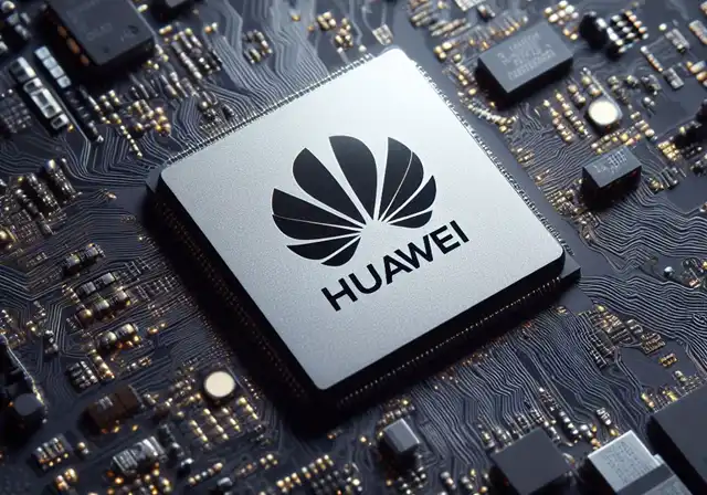
Huawei Bets on Tao’s Law to Reach 1.4nm-Equivalent Chips by 2031 — No EUV Required
Huawei Bets on Tao’s Law to Reach 1.4nm-Equivalent Chips by 2031 — No EUV Required
- Linux Kernel Removes strncpy After Six Years and 362 Patches
- Linux Kernel Drops 40-Year-Old AppleTalk Protocol — AI-Generated Patch Flood Was the Last Straw
- Apple’s Native Linux Container Tool Has Arrived — But Can It Really Replace Docker?
- 60% of MD5 Password Hashes Can Be Cracked in Under an Hour with a Single GPU
- Dirty Frag: Root Access on Every Major Linux Distribution — No Patch, No Warning
Conceptual illustration of Huawei’s Tau (τ) Scaling Law, unveiled at ISCAS 2026 in Shanghai. The framework proposes replacing geometric transistor shrinkage with system-level time efficiency.
Huawei Bets on Tao’s Law to Reach 1.4nm-Equivalent Chips by 2031 — No EUV Required
The Chinese tech giant unveiled a sweeping new chip design framework — the Tau (τ) Scaling Law — at IEEE ISCAS 2026, arguing that “time-constant scaling” can close the gap with TSMC’s leading-edge nodes, even as US sanctions keep EUV lithography tools out of China’s reach.
In a keynote that reverberated across global chip markets, Huawei’s He Tingbo — chairwoman of the company’s Scientist Committee and president of its semiconductor business — stood before researchers and executives at the 2026 IEEE International Symposium on Circuits and Systems in Shanghai and announced a new law to govern the future of chip development.
The principle, formally named the Tau (τ) Scaling Law — rendered in Chinese as “韬定律” — proposes a fundamental pivot: instead of chasing smaller and smaller transistors through geometric miniaturization, chipmakers should focus on compressing signal propagation delay across the entire computing stack. In Huawei’s framing, it is a replacement for Moore’s Law, the half-century-old rule that predicted transistor counts would double roughly every two years.
The practical implication is ambitious: Huawei projects that high-end chips built on this principle will achieve transistor density equivalent to a 1.4-nanometer process node by 2031 — a level analysts expect to represent the global frontier for advanced chipmaking at the end of this decade, when TSMC plans to mass-produce true 1.4nm chips.
What the Tau Scaling Law Actually Claims
It is critical to understand what Huawei is — and is not — saying. The 1.4nm claim is not a statement that China has solved leading-edge photolithography. Huawei openly acknowledges it does not have access to ASML’s extreme ultraviolet (EUV) machines, the tools necessary to print transistors at true sub-3nm geometries. US sanctions have effectively barred these tools from Chinese foundries, and even deep-ultraviolet (DUV) machines face tightened export controls.
Instead, the Tau Scaling Law shifts the benchmark entirely. Rather than measuring progress in gate width — the traditional metric of a process “node” — the framework measures advancement in signal propagation delay reduction across devices, circuits, chips, and systems as a whole. In this multi-level co-optimization view, a chip optimized end-to-end for timing efficiency can deliver real-world performance equivalent to a geometrically smaller chip, even if its individual transistors are physically larger.
We have achieved a series of advances that would be difficult to attain through advanced process technology alone. I used to think it may take us 10 years, but six years — we are here.
— He Tingbo, Huawei Semiconductor Business President, ISCAS 2026
LogicFolding: The Engine Behind the Claim
The concrete architectural innovation underpinning the Tau Scaling Law is what Huawei calls LogicFolding — a 3D chip-stacking approach that layers transistors vertically rather than pushing them closer together horizontally. By folding logic circuits into multiple tiers, the architecture shortens critical-path wiring and dramatically reduces resistive and capacitive (RC) load, the twin enemies of signal speed in dense chips.
The company claims this approach already delivers a 55% improvement in transistor density compared to conventional planar designs at the same process node. Huawei plans to launch a new-generation Kirin smartphone processor fully incorporating LogicFolding technology before the end of 2026 — describing it as “a big leap ahead” and teasing that users will see “the surprise before winter.”
How It Stacks Up Against Global Rivals
The ambition of the 2031 target becomes clearer when set against the global competitive landscape. TSMC, the world’s leading foundry, is widely expected to begin mass-producing true 1.4nm chips around 2028. Samsung and Intel are pursuing similar timelines for comparable nodes. Huawei’s claim is that it can reach equivalent effective performance three years later — not through lithography but through architecture.
Note: Huawei’s metric is effective transistor density via 3D stacking, not photolithographic node. Direct comparisons carry significant caveats as methodologies differ.
The Skeptic’s View: Bold Claim, Unverified Data
Independent semiconductor analysts and international media have greeted the announcement with a mixture of respect and caution. The core skepticism is methodological: Huawei has not released independent performance benchmarks or peer-reviewed data to substantiate its density claims. The 1.4nm-equivalent framing relies on the company’s own definition of “equivalence,” which is not yet validated by third parties.
There are also structural constraints that Tau’s Law cannot fully legislate away. SMIC, China’s premier foundry and Huawei’s primary chip manufacturer, currently operates at a 7nm N+2 class process using multi-patterning DUV — a costly, low-yield workaround that is itself approaching its practical limit. Even 3D stacking and folding architectures must eventually be fabricated somewhere, and the quality of those layers depends on the underlying lithography.
The US export control regime continues to tighten. Restrictions on DUV equipment, EDA software, advanced chip packaging materials, and high-bandwidth memory components create a multi-front challenge that architecture alone may not overcome. Analysts note that Huawei’s six-year track record of producing 381 chip designs is genuinely impressive — but making chips that compete at the bleeding edge of global AI and mobile performance remains a different challenge entirely.
The Huawei 1.4nm claim is not a statement that China has solved leading-edge lithography. It is an attempt to move part of the scaling argument away from gate geometry and towards timing, interconnect and system-level efficiency.
— EE News Europe, May 25, 2026
Why the Announcement Still Matters
Despite the skepticism, the significance of Monday’s announcement should not be understated. This marks the first time a Chinese company has proposed a guiding principle for the global semiconductor industry, an arena historically dominated by Intel’s Pat Gelsinger (coiner of a Moore’s Law extension), TSMC’s foundry roadmaps, and American research institutions.
Markets responded swiftly. Shares in SMIC surged 7.6% following the announcement. Huawei-ecosystem component suppliers — including Meian Sen and Yunding Technology — jumped sharply in early trading as investors bet on a domestic supply chain energized by the new framework.
Huawei’s 2025 annual revenue reached 880.9 billion yuan ($130 billion), a figure built in significant part on its ability to design chips spanning smartphones, AI accelerators, telecommunications, networking, automotive and consumer electronics — all under the constraint of US sanctions. The Tau Scaling Law, whatever its ultimate technical merit, represents Huawei’s declaration that it intends to set, not merely follow, the rules of the road.
He Tingbo closed her keynote with a call that cut against the narrative of technological nationalism: “The semiconductor industry thrives on openness and collaboration. No single company can independently solve the challenges of the industry’s evolution.” Whether the world’s chip leaders are willing to collaborate with a sanctioned Chinese firm on a framework it invented remains, for now, an open question.
What to Watch Next
The autumn 2026 Kirin launch with LogicFolding will be the first real-world test of Huawei’s claims. Independent teardowns and benchmark analyses of that chip will offer the semiconductor community its first hard data point on whether time-constant scaling can genuinely substitute for geometric miniaturization — or whether the Tau Scaling Law remains, for now, a compelling manifesto more than a proven engineering reality.